EN
PCBServices
Intro to 2step HDI+Gold finger PCB supplier & manufacturers CAMTECH PCB

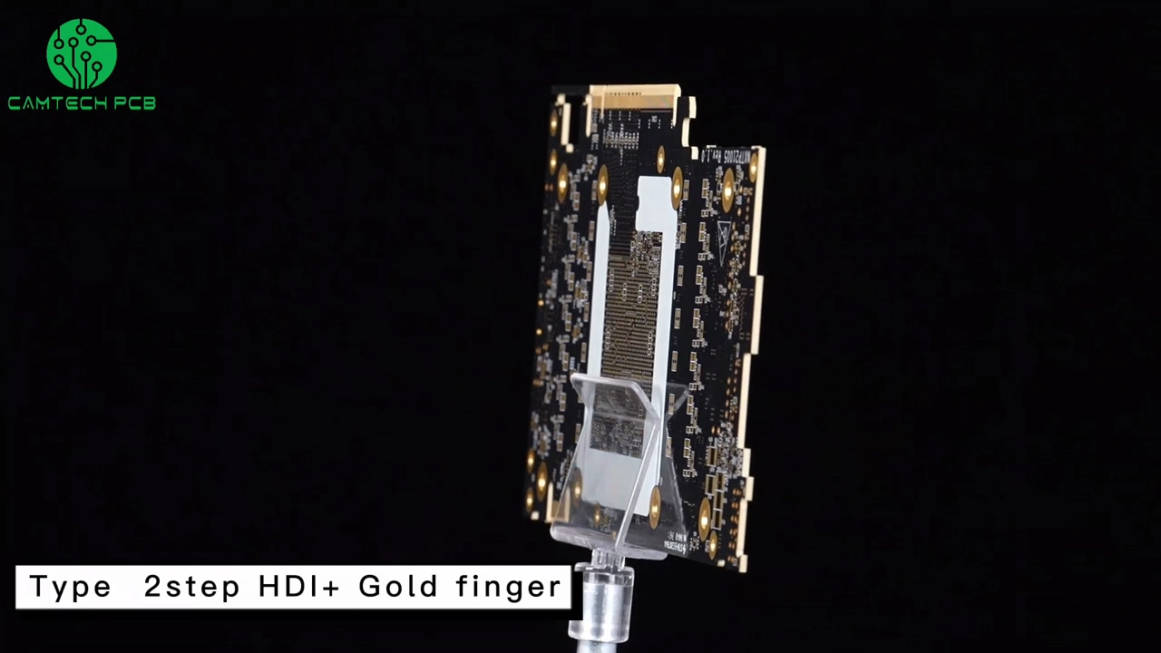
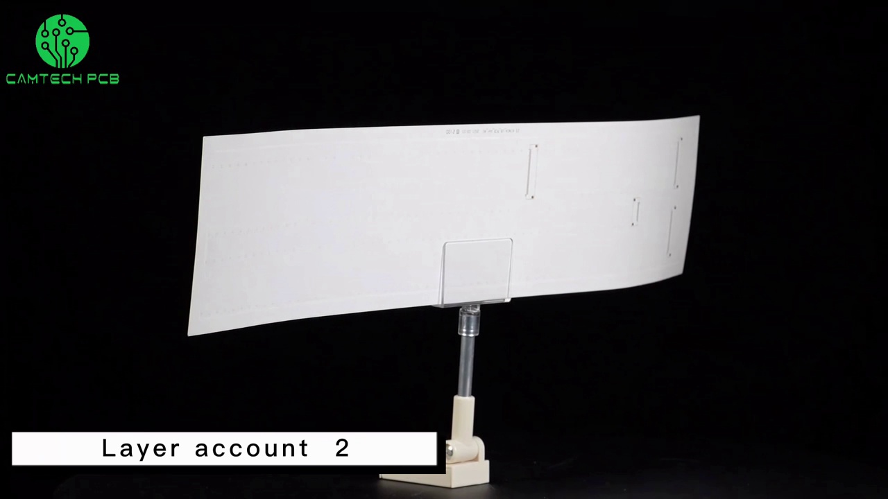
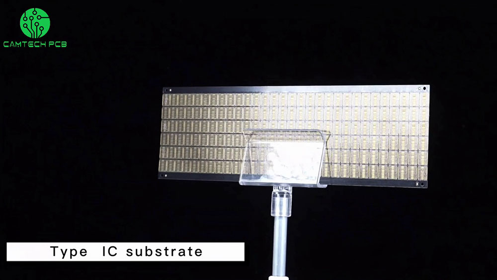
High density interconnects (HDI) PCB, represent one of the fastest-growing technologies in PCBs. Because of its higher circuitry density than traditional circuit boards, the HDI PCB design can incorporate smaller vias and capture pads, and higher connection pad densities. HDI Boards contain blind and buried vias and often contain micro vias of 0.006 or less in diameter.


By using HDI technology, designers now can place more components on both sides of the raw PCB if desired. Now as the development of via in pad and blind via technology, it allows designers to place smaller components closer together. This means faster transmission of signals and a significant reduction in signal loss and crossing delays.


Intro to 2step HDI+Gold finger PCB supplier & manufacturers CAMTECH PCB
Products Information
Zipper closure 1/5 zip athletic pullovers for men. Stretchy, lightweight, fast-drying fabric for superior performance. REGULAR FIT - US standard sizes. An athletic fit that sits close to the body for a wide range of motion, designed for optimal performance and all day comfort. FEATURES - Quarter zip closure;Thumbholes on long sleeves to keep them in place during workout

HDI PCB is frequently found in mobile phones, touch-screen devices, laptop computers, digital cameras, 4G network communications, also prominently featured in medical devices.


Advantages of HDI PCB

The most common reason for using HDI technology is a significant increase in packaging density. The space obtained by finer track structures is available for components. Besides, overall space requirements are reduced will result in smaller board sizes and fewer layers.

Usually FPGA or BGA are available with 1mm or less spacing. HDI technology makes routing and connection easy, especially when routing between pins.


Function improved by HDI PCB:

1.Denser trace routing

2.More stable power

3.Reduce interference inductance and capacitance effects

4.Improve signal integrity in high-speed design


Accelerate Development with HDI Printed Circuit Boards

1.Easier to place SMD components

2.Faster routing

3.Reduce frequent relocation of components

4.More component space (also by Via-in-Pad)

Related Products
CONTACT
Submit A Request
When your product is still in the design stage, we are very willing to participate in your product design, and our engineers will give you advice on the design, performance, cost of PCB to help you reduce the cost of PCB and provide valuable help to bring your product to market quickly and successfully.

Contact : Mr. Zhu

Market center :

Room 916, Huafeng International Building, No. 4018 Baoan Avenue, Baoan District, Shenzhen, Guangdong, China 518102

Phone : +86-13713989501

Email : info@camtechcircuits.com
WILLKOMMEN ZUR BERATUNG!
ingYuan factory:
M1-04 and 05A, YingFu Industrial Area Anfeng Industrial Park,QingYuan High-Tech Development Zone,QingYuan City, Guangdong Province, China ZhuHai factory:
No.1388, Qixing Avenue, Fushan Industrial Park, Qianyuan Town, Doumen District, Zhuhai City ,Guangdong, China

Datenschutzerklärung
SCHNELLE LINKS
Home
PCBServices
Markets We Serve
Case Studies
Factories
About Camtech PCB
Contact Us
PCB-DIENSTLEISTUNGEN
PCB Services
High TG PCB
HDI PCB
Flexible PCB
Aluminum PCBs
High-Frequency PCB
OTHERS
Thick Copper PCB
Multilayer PCB
SMT STENCILS
KONTAKTIEREN SIE UNS
Email: info@camtechcircuits.com
Tel.: +86 13713989501
WeChat: +86-13713989501

Add:
Hongkong Add: Room 023 9/f Block G Kwai Shing Ind Bldg (stage 2)42-46 Tai Lin Pai Rd Kwaichung Nt

Room 916, Huafeng International Building, No. 4018 Baoan Avenue, Baoan District, Shenzhen, Guangdong, China 518102
Untersuchung
KONTAKTIEREN SIE UNS
Kontaktieren Sie uns