Tel: +86-13713989501
Email: info@camtechcircuits.com
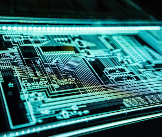
Heavy Copper PCB or calls Power Supply PCB is manufactured with copper weights anywhere between 3-20oz/ft2, Copper weights above 20oz/ft2 are also possible and are referred to as extreme copper. the increased copper weight combined with a suitable substrate and thicker plating for the through holes transforms the once unreliable,weak PCB into a durable and reliable wiring platform. Now various power electronics products are being designed every days for a range of applications: such as Power line monitors, High power rectifiers, planar transformers, and power convertors,etc.
Heavy copper PCB used for High power and high current circuits and their control circuits were designed or produced separately on separate PCB. Heavy Copper PCB makes it possible to integrate high current circuits and control circuits to realize a highly dense, in a simple board structure,also the advantages include reduced layer count,low impedance power distribution,smaller footprints and potential cost savings.The features of Heavy Copper PCB can be seamlessly connected to normal PCB, The board incorporating Heavy Copper PCB are produced in the same way, albeit with specialized etching and plating techniques, such as high speed/step plating and heavy copper differential etching.
The main reason to choose something is the number of advantages they provide and their wide range of uses. Well, thick copper PCB offers a number of uses and benefits that make our life easier and products better. We have listed a number of benefits below:
◈ Higher resistance to thermal stress
◈ An increase in the current load
◈ Increased mechanical strength at conductor sites and PTH holes.
◈ Usage of exotic materials to their full potential (i.e., at high temperature) without interrupting the circuit.
◈ Reduce the size of the product by incorporating several weights of copper in the same circular layer.
◈ Heavy copper panels carry higher current through the plate and help transfer heat to the external heat sink.
◈ High power density on-board transformers.
Heavy copper board helps to transfer heat to external radiator and transfer higher current.
Heavy copper board can support high current frequency, repeated thermal cycle and high temperature
Heavy copper board reduces the chance of circuit failure.
Heavy copper board PTH hole and connector have high mechanical strength.
Heavy copper board can carry large current.
The part with a large amount of copper deposits on the Heavy copper board can be used as a radiator. Alternatively, you can connect it to a cold board.
1. Pay attention to the copper filling level of the inner layer. The reason for this is to avoid very low copper fill levels. If this happens, when the resin content is low, there will be gaps between the layers and delamination will occur.
2. It is better to select the quantity and type of prepreg by using software that can help you to realize multi-layer combination design.
3. Electroplated coating is very important. Considering that you are designing heavy copper PCB, you will use more plated copper.
4. Ensure that the layers of your solder resist are thick. That way, you’ll adequately guard the mosaic edges. For instance, your final circumferential thickness should have a value of at least 0.25mm higher than its initial thickness.
◈ Your heavy copper PCB manufacturer Camtech PCB
One thing is certain about heavy copper PCB - it requires special technology to achieve the best results. Although there are various difficulties in the manufacturing process, we provide quality at the most favorable price.
At the same time, we have been engaged in this business for many years. Therefore, you can rely on our experience to build the best PCB according to your specifications. Our professional knowledge is not only to give you professional guidance, we can flexibly handle small batch to large batch of circuit board manufacturing. During this period, we are always committed to following strict quality standards
How Thick Is The Copper On The PCB?
How To Select The Thickness Of PCB Copper?
How To Remove Unwanted Copper From PCB During Manufacturing?
Why Does PCB Use Copper?
What Is The Weight Of Copper Base?
What Should Be Considered For The Layout Of Thick Copper PCB?
What Else Should We Pay Attention To For The Standard Characteristics Of Heavy Copper?
What Should Be Considered In PCB Industry From Common Design To Heavy Copper PCB Manufacturing?
Should I Choose Ordinary Circuit Board Or High Current Circuit?


