Zipper closure 1/5 zip athletic pullovers for men. Stretchy, lightweight, fast-drying fabric for superior performance. REGULAR FIT - US standard sizes. An athletic fit that sits close to the body for a wide range of motion, designed for optimal performance and all day comfort. FEATURES - Quarter zip closure;Thumbholes on long sleeves to keep them in place during workout
FAQ
1.Can you doing the HDI board in one week?
Yes, we can doing the HDI board in one week.
2.Can you ship the PCB door to door?
Yes, we can ship the PCB door to door and quickly
3.Can you do quick turn prototyping?
Yes, we can do quick turn prototyping and receive urgent order.
Advantages
1.We can do Multilayer, HDI and Roger such difficult board.
2.The capacity of our factory is more than 1500,000 m².
3.We have the Certificate of ISO 9001, US & Canada UL certificates, TS 16949 & RoHS compliance.
4.We have quick delivery time, 2 days can reach to USA and Europe.
About CAMTECH PCB
CAMTECH PCB is an international, professional and reliable PCB supplier located in Shenzhen and Zhuhai city. They focus on exporting PCBs mainly to European and North American market. CAMTECH PCB wаѕ established in 2002, has three modernization PCB and FPC factories. We have more than 3000 workers, the annual output capacity is more than 1500,000 m². Based on our extended experience and technology , we are able to offer customer one-stop service with small, medium and mass production. By good quality and delivery assurance, we can meet with all customer's request. Our products are widely applied in security, industrial control, communication, medical instrument and automotive electronics etc. G CAMTECH PCB has passed the certificates of international quality system as ISO 9001, US & Canada UL certificates, TS 16949 & RoHS compliance. We also cooperate with world famous PCB manufacturer, perfect our supply chain constantly. We are capable of providing various PCB services, such as1-30L through-hole board & HDI. We are pursuing to offer best services and competitive good prices to our customer. And striving to provide best solution of lead time, quality & after-sales services. We take standard working instruction program, set up a perfect training plan.
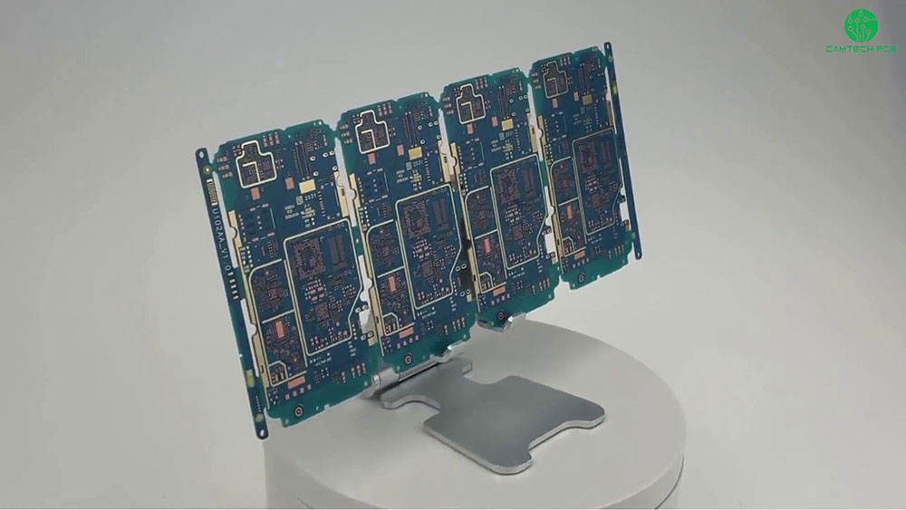
What is HDI Board
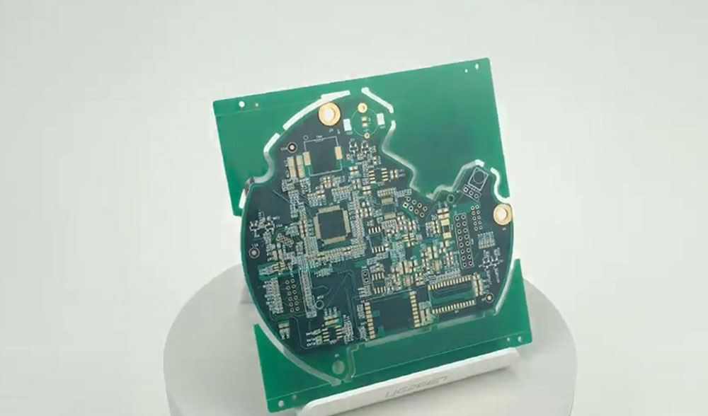
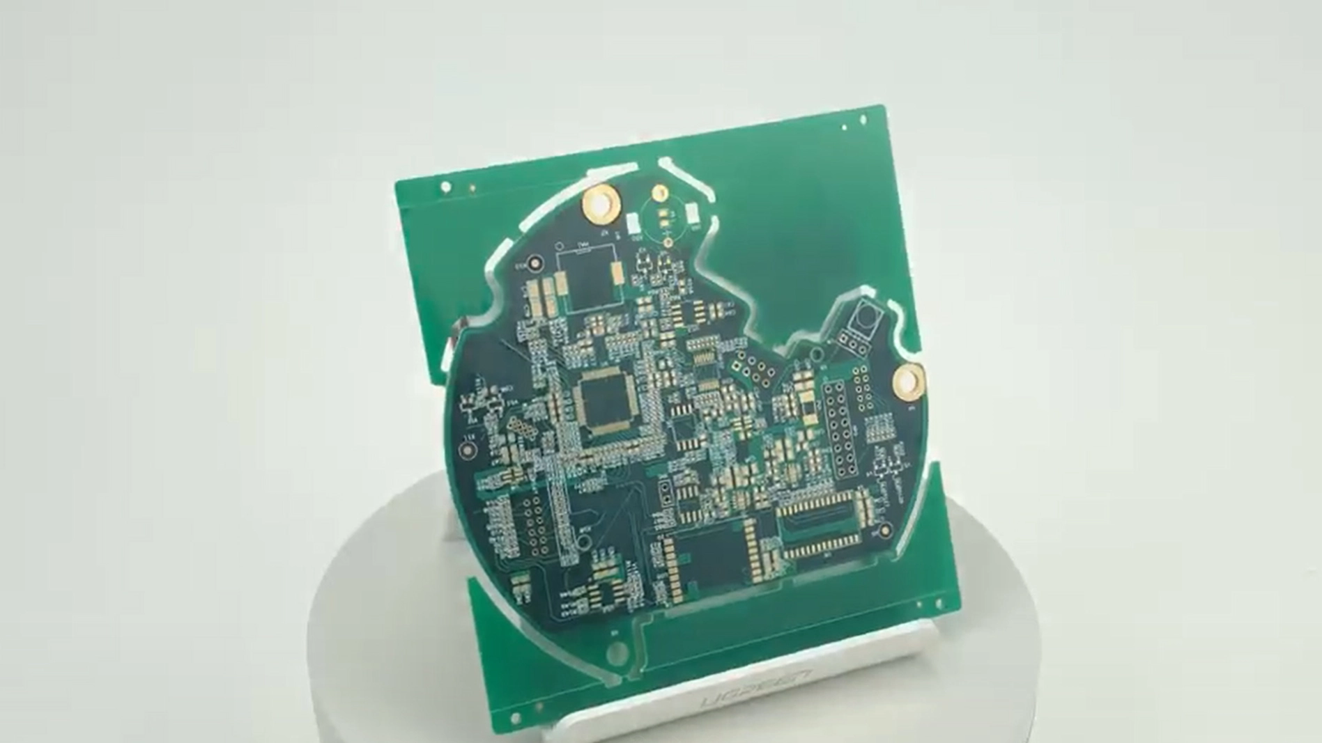
High density interconnects (HDI) PCB, represent one of the fastest-growing technologies in PCBs. Because of its higher circuitry density than traditional circuit boards, the HDI PCB design can incorporate smaller vias and capture pads, and higher connection pad densities. HDI Boards contain blind and buried vias and often contain micro vias of 0.006 or less in diameter.
By using HDI technology, designers now can place more components on both sides of the raw PCB if desired. Now as the development of via in pad and blind via technology, it allows designers to place smaller components closer together. This means faster transmission of signals and a significant reduction in signal loss and crossing delays.
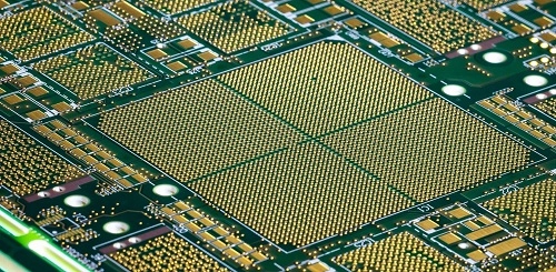
Advantages of HDI PCB
The most common reason for using HDI technology is a significant increase in packaging density. The space obtained by finer track structures is available for components. Besides, overall space requirements are reduced will result in smaller board sizes and fewer layers.
Usually FPGA or BGA are available with 1mm or less spacing. HDI technology makes routing and connection easy, especially when routing between pins.
Function improved by HDI PCB:
1.Denser trace routing
2.More stable power
3.Reduce interference inductance and capacitance effects
4.Improve signal integrity in high-speed design
Accelerate Development with HDI Printed Circuit Boards
1.Easier to place SMD components
2.Faster routing
3.Reduce frequent relocation of components
4.More component space (also by Via-in-Pad)
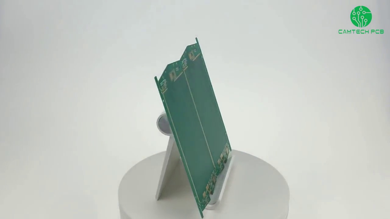
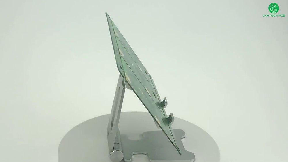
Product details
FAQ
Is your PCB board with good quality?
Yes, our PCB board is with good quality, and we double test the board before ship it.
Can you doing the HDI board in one week?
Yes, we can doing the HDI board in one week.
What kind of boards are you good at?
We are good at Multilayer, HDI and Rogers such board.
Can we visit your factory?
Yes, you can visit our factory any time.
Can you do quick turn prototyping?
Yes, we can do quick turn prototyping and receive urgent order.
Our services
1.Oem or odm are acceptable.
2.We accept small order/trial order for customer to check whether the products is suitable for the market.
3.Will be available online almot in 24 hours service for your esteemed company.
4.We are glad to hear from you soon and to start a business relationship with your esteem company.
If you have another questions,please feel free to contact us.