Tel: +86-13713989501
Email: info@camtechcircuits.com
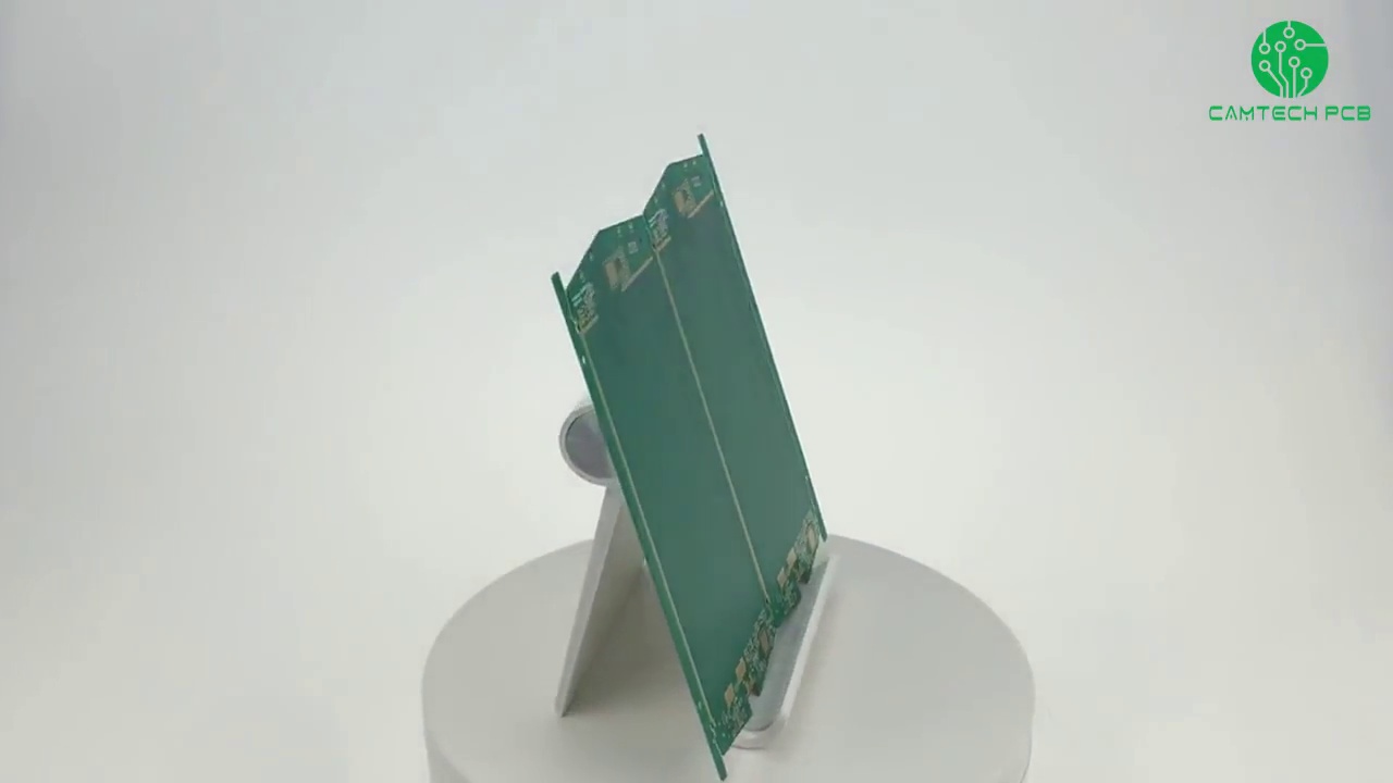
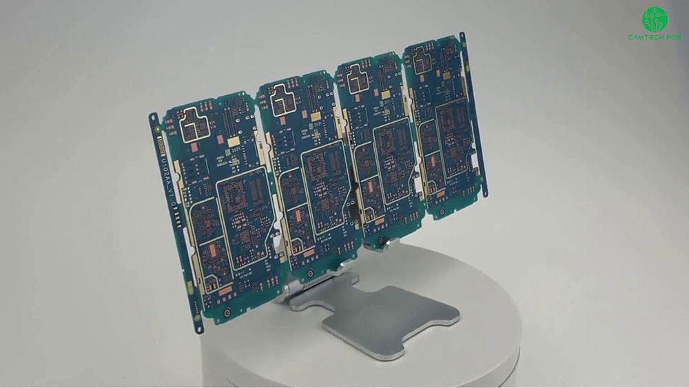
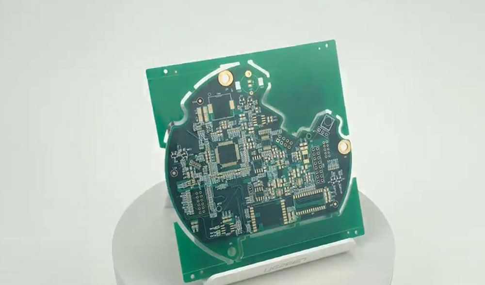
Product parameters:
Number of layers: 8 layers
PCB or FPC: PCB
Material: FR4 TG>170 , halogen-free
Finished thickness: 0.9MM
Surface copper thickness : Inner layer/outer layer completed surface copper pressure ≥15um
Copper thickness in the hole: through hole/buried hole/blind hole copper thickness ≥10um
Inner layer line width/line spacing: 2/2.95MIL, outer layer line width/line spacing: 2.95/2.95MIL
BGA solder size: 0.2MM
Minimum aperture: laser 0.1MM, through hole 0.1MM
Color : soldermask blue, silk screen white
Surface Finish : immersion gold
Immersion gold thickness: 2U ”
Product details: 8-layer anylayer connected HDI, resin hole plugging, electroplating filling, small line width and line spacing
1. HDI optional interconnection material selection
Choose high TG Halogen-free board allows it to withstand multiple pressings to control expansion and contraction, and cannot burn at high temperatures and can only soften ( TG refers to the glass transition temperature, which is the glass transition temperature of the board when heated at high temperatures, generally TG The plate temperature is above 130 degrees, high TG is generally greater than 170 degrees, and medium TG is approximately greater than 150 degrees );
2. HDI arbitrary interconnection technology
anylayer connected HDI board allows it to accommodate more electronic components, allowing the construction of more complex circuit systems. It has the advantages of high integration, high-speed transmission, miniaturization, energy saving and environmental protection.

3. Resin plugging and electroplating filling
When the pad spacing of the BGA package is too small to allow wiring, it is necessary to design a hole in the disk, drill the hole on the pad, and route the wiring from the inner layer or the bottom layer. At this time, the hole in the disk needs to be plugged with resin and electroplated. Filling, if the hole in the pad is not plugged with resin, it will lead to poor welding during welding, because there is a small hole in the middle of the pad and the soldering area is small, and tin will leak in the hole ;
4. Assist customers to optimize drilling
This board contains a variety of blind hole designs, and the diameter of the through-hole blind holes is 0.10mm. It is recommended that customers change all PTH holes to a stacked hole design (including through holes) (a hole disk will be added to the inner layer). After optimization, it will be laser Blind holes stacked on buried holes (for example: 3-6 blind holes are changed to 3-4 laser holes stacked on 4-5 buried holes stacked on 5-6 laser holes), and all laser holes are filled with hole plating.
This board has designed many blind holes. and all the size are 0.10mm, suggests Customer to all the PTH holes (contain outlayer through-hole) (the annular ring will added in inner layer) optimizing to overlapping hole (EX: the 3- 6 blind holes divide into 3-4 laser holes overlap 4-5 buried holes overlap 5-6 buried holes. and all the laser holes will plug with copper.