Tel: +86-13713989501
Email: info@camtechcircuits.com

Principais características da placa de circuito de alta frequência
◈ Small and stable. In addition, there is no delay in signal transmission. Ideal for signal transmission. And effectively reduce signal
waste. The copper free foil separates with temperature change.
◈ HF board with low water absorption.
Impressive properties such as impact resistance, heat resistance, peel resistance and chemical resistance. In addition,
the high peel resistance improves the signal quality of PCB.
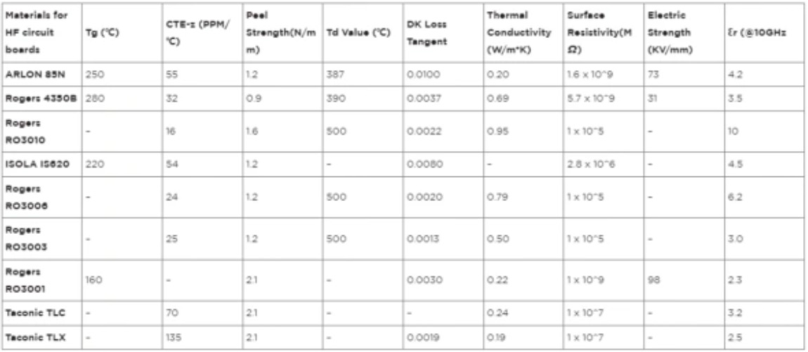
Materials required for high frequency circuit boards
◈ Because high-frequency PCB layouts work at high frequencies, they often suffer from extremely high temperatures.
◈ If the material is unsuitable, it may lead to thermal stress accumulation. Therefore, we need to choose a material with
a good coefficient of thermal expansion (CTE). In addition, the material shall have high dimensional stability.
This way it will not be degraded at runtime.
◈ We usually use these materials for advanced applications.
Therefore, the materials we use for manufacturing should have excellent thermal conductivity and electrical conductivity.
◈ We often deploy high-frequency PCB in extreme environments. Therefore, they should have high corrosion resistance and moisture resistance.
Therefore, the materials we use to make high-frequency PCB should be moisture-proof. High frequency signals are very sensitive to noise.
Therefore, we need to use materials with stricter impedance tolerance to manufacture these PCBs.
◈ Reduce moisture content
When moisture is involved, a small amount will distort the electrical performance of the high-frequency board. Interestingly,
compared with traditional FR-4, the humidity level of PTFE and other materials is as low as 2%. The rating of FR-4 is very high, about 50%. As a result,
the reduced moisture content translates into significant electrical performance.
◈ Excellent thermal management
Most of the time, high-frequency PCB will generate a lot of heat during operation. Therefore, with polyimide and other
materials, you can rest assured that you will obtain strong thermal performance. In addition, you can use them in harsh environments.
◈ It has a controlled impedance
The board contains materials that maintain a Dk tolerance of /- 2% or more. This means it is
very useful for circuits that require strict impedance control. Most of the time, high
◈ Comprehensive and excellent signal performance
Because of its PTFE material, the dissipation factor is low. This also means that it reduces signal loss.
◈ It has dimensional stability
High frequency PCB has thermosetting hydrocarbon material. These materials promote mechanical stability.
◈ High frequency PCB design and layout
Surface treatment of high-frequency copper foil
As the frequency increases, the signal flows through the orbit.
The track generates current. The current then pushes the current density toward the outer surface, not toward the center of the track. Therefore,
during the production process, you may encounter an increase in copper surface roughness. As a result, there will be a lot of signal loss at high frequencies.
Resistance welding layer under high frequency
The solder mask has a high dissipation factor. Therefore, when you apply it to high-frequency traces, it increases
the dielectric loss of the circuit.
How to produce controllable impedance transmission line?
Controlled impedance is created to
avoid signal loss. There are two simple ways to achieve this:
◈ Microstrip Method
This method is related to tracing at the top level. The routing usually has a ground plane below it.
The calculation involved in this method is quite complex. In addition, it depends on different factors, such as the height above the plane,
the relative dielectric constant, the line width, etc. Therefore, your best choice is to ensure that your ground plane is very close to the top layer
◈ Stripline Method
The stripline method is similar to the microstrip line, the only difference is that the stripline has an additional group plane. The group plane is
above the trace. When using this method, be sure to place the route between two planes. This method is a better choice. The reason is that there is EMI radiation in two planes.
|
Plate thickness |
0.4 – 5.0 mm |
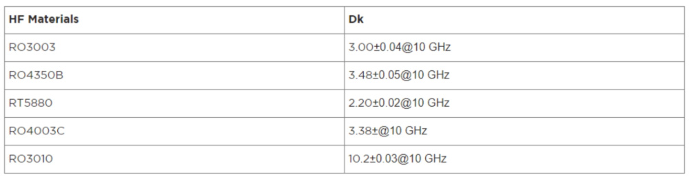
Materials |
RO3010, RO4350B, RT5880, RO4003C, RO3003 |
|
Polypropylene |
Domestic - (6700), Rogers 4450F, etc |
Order quantity |
No MOQ |
|
Screen printing surface |
It depends on the document. |
Color of solder mask |
Blue, red, yellow, green, white |
|
Number of floors |
2 – 40 |
Quality grade |
Standard IPC 2 |
|
Alternative methods |
Countersink, gold finger, peelable soldering tin, mask carbon oil |
Plate size |
0.4-5.0 mm |
|
Silk screen color |
black, yellow, white |
Minimum drilling diameter |
0.15 mm |
|
Surface treatment |
Tin deposition – RoHS, ENIG – RoHS, gold plating – RoHS, silver deposition – RoHS |
Weight of finished copper |
0.5 – 2.0 0z |
|
Manufacturing time |
This depends on the project (10 days to 5 weeks) |
Minimum ring |
0.1 mm |
|
Minimum tracing |
3mil/3mil |
Impedance tolerance |
± 10% |
How To Select High Frequency Pcb/High Speed PCB Materials?
How To Deal With The Signal Integrity Problem In High-Frequency Signal Transmission?
What Should Be Considered In High-Frequency PCB Design/High-Frequency Design?


